Customized Biosensor Interfaces Service
Enhance Your Research with Advanced Customized Die-Level CMOS Biosensor Post-Processing - Swiss Made
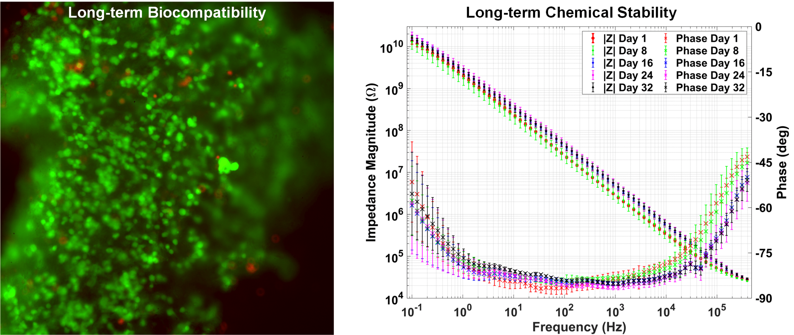
With over 10 years of research and experience, we have developed comprehensive in-house post-processing technologies at ETH Zurich's IDEAS group, which enable customized electrode construction, metallization, passivation, and surface molecular functionalization directly on biosensors and bioelectronics integrated circuit (IC) chips. Our ETH IDEAS in-house post-processing capabilities support die-level IC samples including CMOS ICs, cover a vast range of metallic and dielectric materials, and ensure long-term biocompatibility, sealing, and electronic interface integrity in biological media.
To benefit the research community, we offer a non-profit service of customized post-processing and surface functionalization of bioelectronics and biosensor IC chips from researchers and technologists both within Switzerland and worldwide. As your partner, we are committed to supporting your technical demands and research successes with Swiss precision, quality, and reliability.
How does it work? You send us your IC chips with your requirements. We post-process and/or surface functionalize your chips and send them back to you.
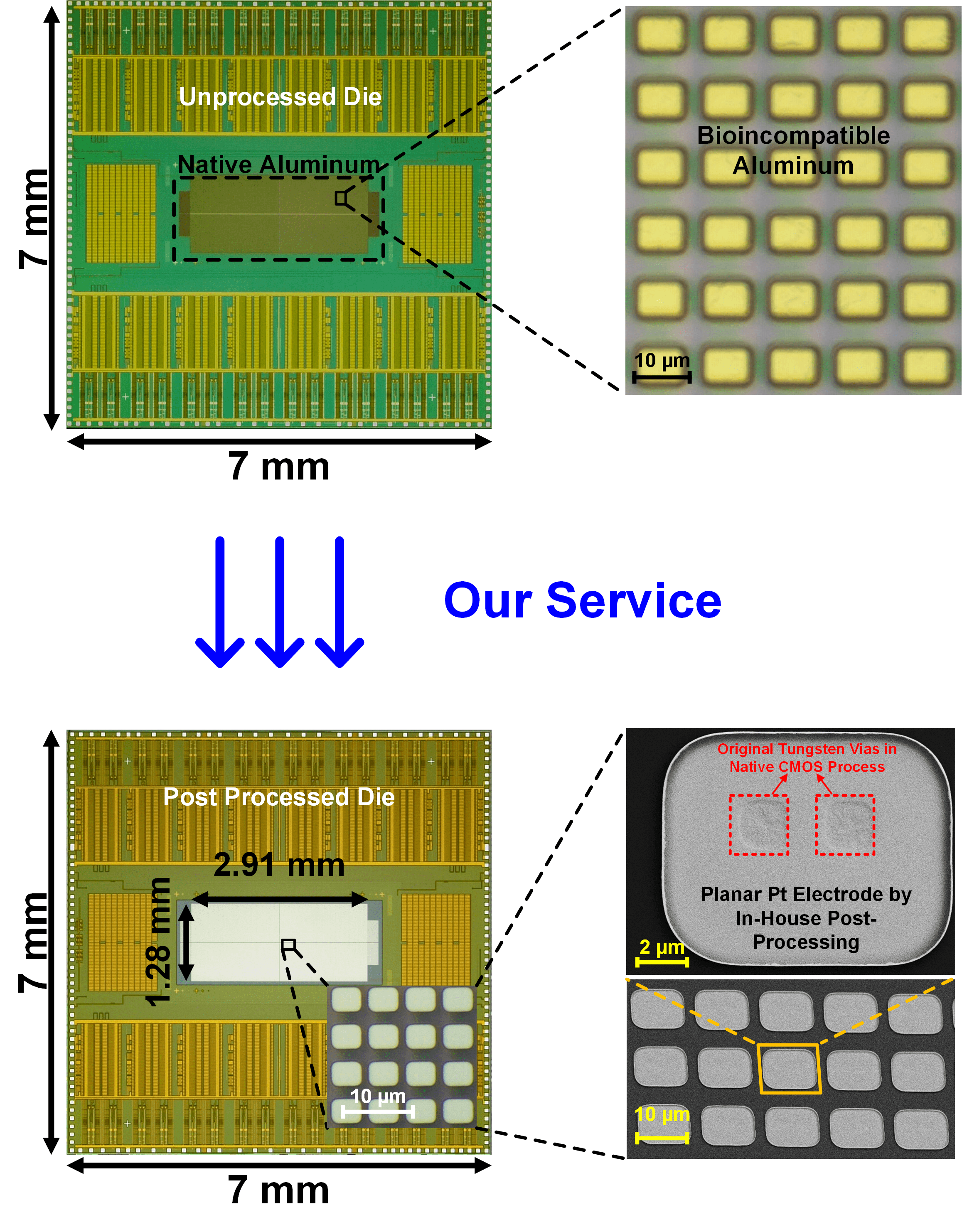
Before and After: The Transformation of A CMOS Array Chip
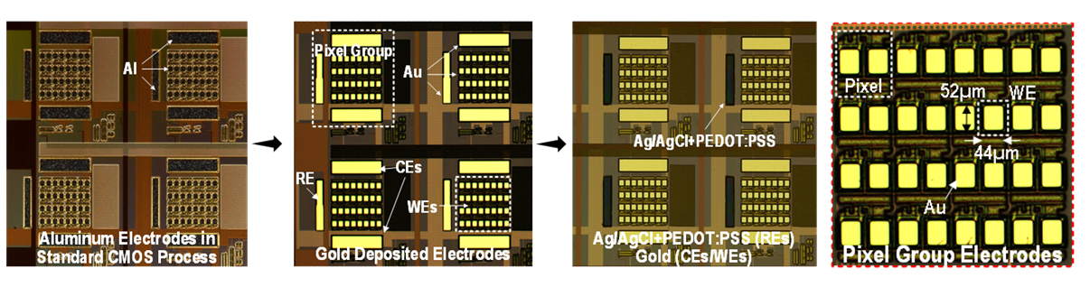
Below are the images for a CMOS Joint Cellular/Molecular Biosensor Array Chip before and after our in-house post-processing steps. The native aluminum pads on a single 7mm×7mm CMOS chip are removed, and new planar Ti/Pt electrodes (11μm×8.84μm) are formed to connect the original Tungsten vias and the underlying CMOS electronic circuitry. An array of total 24k Ti/Pt electrodes is built on the CMOS chip with 100% success rate. Our service also covers a wide variety of other metallic or dielectric electrodes.
Services Offered
We offer bespoke IC post-processing service, including but not limited to:
- IC die-level post processing (for single CMOS dies down-to 5mm x 5mm/chip)
- Removing top back end of line (BEOL) layers for IC chips including top passivation, dielectric layers, and metallization/via layers.
- Elimination of native CMOS Aluminum electrodes and replacing them with customized electrode materials.
- Building customized electrode array on-chip with tailor-made shape and sizing (down-to 4.5um x 4.5um) for single-cell resolution or tissue-level analysis.
- Material selection for customized electrodes including but not limited to Au, Pt, Carbon, TiN, Ir, Pd, W.
- Rebuilding customized top metallization, dielectric, passivation layers on IC chips with design flexibility beyond standard CMOS fabrication limitations.
- Surface functionalization on electrodes and/or top passivation such as PEDOT:PSS, Ionophore-based membranes for ion selective sensing (K, Na, Ca), Parylene, etc.
Partner with us to see your research vision come to life, from conceptual design to the final technology demonstration!
Transparent Pricing: Tailored to Your Research Needs
For detailed pricing information and to discuss your project's specific requirements, please contact us. We're here to guide you through our flexible pricing options and help you find the best solution for your research budget.
Contact Us
Relevant Publications
[1] A. Wang, Y. Sheng, W. Li, D. Jung, G. Junek, H. Liu, J. Park, D. Lee, M. Wang, S. Maharjan, S. Kumashi, J. Hao, Y. Zhang, and H. Wang, "A Multimodal and Multifunctional CMOS Cellular Interfacing Array for Digital Physiology and Pathology Featuring an Ultra Dense Pixel Array and Reconfigurable Sampling Rate," IEEE Transactions on Biomedical Circuits and Systems, pp. 1-18, 2022.
[2] A. Wang, Y. Sheng, W. Li, D. Jung, G. Junek, D. Lee, M. Wang, S. Maharjan, J. Park, S. Kumashi, J. Hao, Y. S. Zhang, K. Eggan, and H. Wang, "A CMOS Cellular Interface Array for Digital Physiology Featuring High-Density Multi-Modal Pixels and Reconfigurable Sampling Rate," in 2022 IEEE International Solid- State Circuits Conference (ISSCC), 2022, vol. 65, pp. 202-204.
[3] S. Kumashi, D. Jung, J. Park, S. Sanz, S. Grijalva, A. Wang, S. Li, H. C. Cho, C. A.-Franklin and H. Wang "A CMOS Multi-Modal Electrochemical and Impedance Cellular Sensing Array for Massively Paralleled Exoelectrogen Screening," IEEE Trans. Biomed. Circuits Syst., vol. 15, no. 2, pp. 221 - 234, Mar. 2021.